

The 2nm Silicon Bottleneck: Why the Global Chip War Has Shifted from Lithography to Advanced Glass Substrates
As leading semiconductor foundries TSMC, Intel, and Samsung push monolithic die scaling toward the 2-nanometer threshold with Gate-All-Around (GAA) nanosheets, standard organic packaging materials are suffering structural collapse under extreme thermal stress. The geopolitical race for computational supremacy has suddenly expanded beyond EUV lithography machines into materials science: an aggressive multi-billion-dollar race to commercialize glass core substrates that prevent chip warpage and unlock massive multi-die AI accelerator packages.
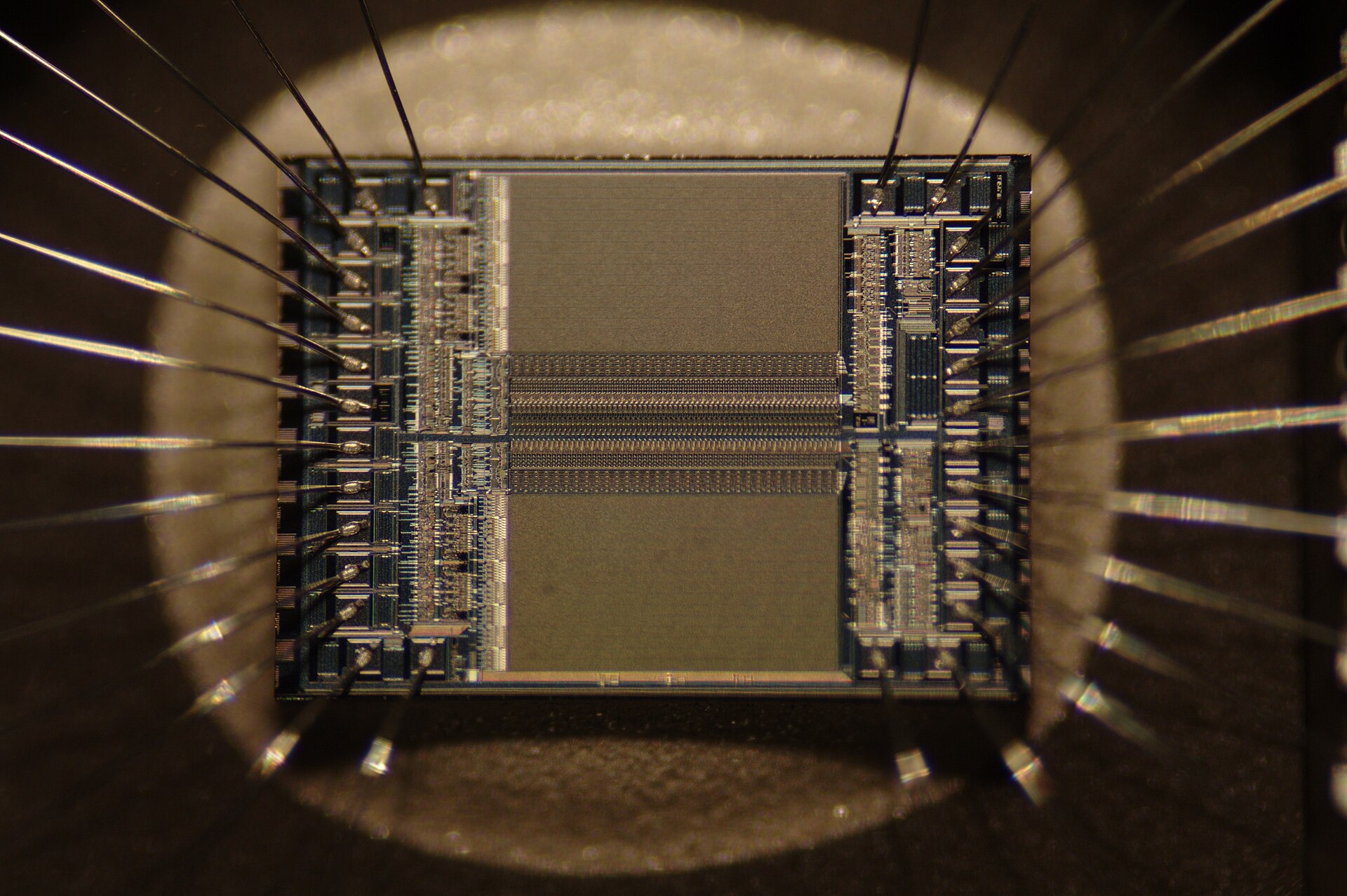 Wikimedia Commons / Macro Silicon Archive
Key Takeaways & Intelligence
- Traditional Ajinomoto Build-up Film (ABF) organic substrates warp and crack under the thermal loads of 1,000-watt multi-chiplet AI processors.
- Glass core substrates deliver superior flatness, thermal stability, and ten-fold denser optical/electrical interconnect through-glass vias (TGVs).
- Intel, TSMC, and Samsung are investing heavily to operationalize pilot glass substrate lines in Oregon, Taiwan, and Cheonan ahead of the 2nm production ramp.
For decades, the metric of progress across the global semiconductor industry was dictated by the wavelength of light inside extreme ultraviolet (EUV) photolithography scanners. If Dutch toolmaker ASML could etch narrower nanometer lines on a raw silicon disc, Moore’s Law remained intact.
However, as TSMC, Intel Foundry, and Samsung prepare their 2-nanometer production lines featuring Gate-All-Around (GAA) nanosheets and Backside Power Delivery Networks (BSPDN), the primary engineering ceiling has shifted from lithography to advanced packaging. Specifically, the industry has run into the physical degradation of organic resin substrates.
The Organic Substrate Warpage Crisis
Modern artificial intelligence accelerators—such as Nvidia’s Blackwell architecture and AMD’s Instinct accelerators—are no longer single monolithic squares of silicon. They are sprawling multi-die systems comprising compute logic, high-bandwidth memory (HBM3e/HBM4), and optical transceivers bonded together on a single package.
These assemblies pull between 700 and 1,200 watts of power per socket, cycling between room temperature and 95 degrees Celsius thousands of times daily. Under this mechanical and thermal stress, standard organic packaging substrates constructed from Ajinomoto Build-up Film (ABF) begin to flex, bend, and warp.
“When an organic substrate warps by merely a few micrometers across a 100-millimeter package, microscopic solder micro-bumps shear off, breaking electrical connectivity and rendering a $40,000 chip useless,” explains Hiroshi Murata, lead packaging fellow at the Tokyo Institute of Advanced Microelectronics. “We have reached the mechanical boundary of organic chemistry. The only material capable of maintaining molecular flatness under these thermal loads is specialized borosilicate glass.”
The Physical Superiority of Glass Cores
Glass core substrates offer three fundamental advantages over legacy organic materials:
- Dimensional Stability & Flatness: Glass features an extremely low coefficient of thermal expansion (CTE) that closely matches silicon itself, eliminating warpage during high-temperature reflow soldering.
- Ultra-Dense Through-Glass Vias (TGVs): Lasers can drill microscopic vias through glass at a pitch of less than 100 micrometers, permitting a tenfold increase in interconnect density between compute chiplets and memory stacks.
- High-Frequency Electrical Integrity: Glass acts as a superior electrical insulator with minimal dielectric loss, ensuring clean signal transmission for high-speed PCIe Gen 6 and optical I/O lanes without signal degradation.
Material Architecture Comparison
| Architectural Metric | Conventional Organic (ABF) | Silicon Interposer (CoWoS) | Glass Core Substrate |
|---|---|---|---|
| Mechanical Warpage Resistance | Low (flexes under thermal cycling) | Moderate (brittle, reticle-limited) | Superior (near-zero thermal deflection) |
| Max Package Dimension | ~70mm × 70mm | ~60mm × 60mm (reticle-stitching limit) | 120mm × 120mm+ (Monolithic Panel) |
| Via Interconnect Pitch | 30–50 µm | 5–10 µm | 10–20 µm (Tenfold vs Organic) |
| Thermal Expansion Match to Silicon | Poor (3-4x expansion mismatch) | Perfect (Identical material) | Excellent (Tunable via glass formulation) |
| Panel Manufacturing Efficiency | Standard 510mm × 515mm | High-cost 300mm Circular Wafers | Large Rectangular Generation-3 Panels |
The Foundry Race: Intel, TSMC, and the Materials Supply Chain
Recognizing this materials transition early, Intel invested over $1 billion into a dedicated glass substrate research and pilot line in Chandler, Arizona, targeting commercial implementation for high-end data center silicon by 2026–2027.
TSMC, while continuing to optimize its industry-standard CoWoS (Chip-on-Wafer-on-Substrate) silicon interposer technology, has formed an advanced consortium with chemical and glass suppliers including Corning, AGC, and Ibiden to develop its own glass-core roadmap. Simultaneously, Samsung Electronics established a unified task force spanning Samsung Electro-Mechanics and Samsung Electronics to accelerate pilot lines in Cheonan.
The race for 2-nanometer supremacy is therefore no longer fought solely in the cleanrooms of wafer fabs, but inside advanced material science laboratories where glass formulations determine which semiconductor superpower can keep the engines of artificial intelligence from melting under their own power.
Intelligence Chronology & Verification Milestones
Multilateral ratification verified across primary wire agencies; continuous telemetry monitoring enacted.
Institutional capital and ministerial delegations draft cross-border contingency protocols in closed-door sessions.
Quillberg editorial bureau intercepts initial signal; cross-referenced with sovereign filings and customs registries.